- 您现在的位置:买卖IC网 > Sheet目录1997 > ICS670M-04ILF (IDT, Integrated Device Technology Inc)IC BUFFER/MULTIPLIER ZD 16-SOIC
ICS670-04
LOW PHASE NOISE ZERO DELAY BUFFER AND MULTIPLIER
ZDB AND MULTIPLIER
IDT / ICS LOW PHASE NOISE ZERO DELAY BUFFER AND MULTIPLIER 4
ICS670-04
REV E 051310
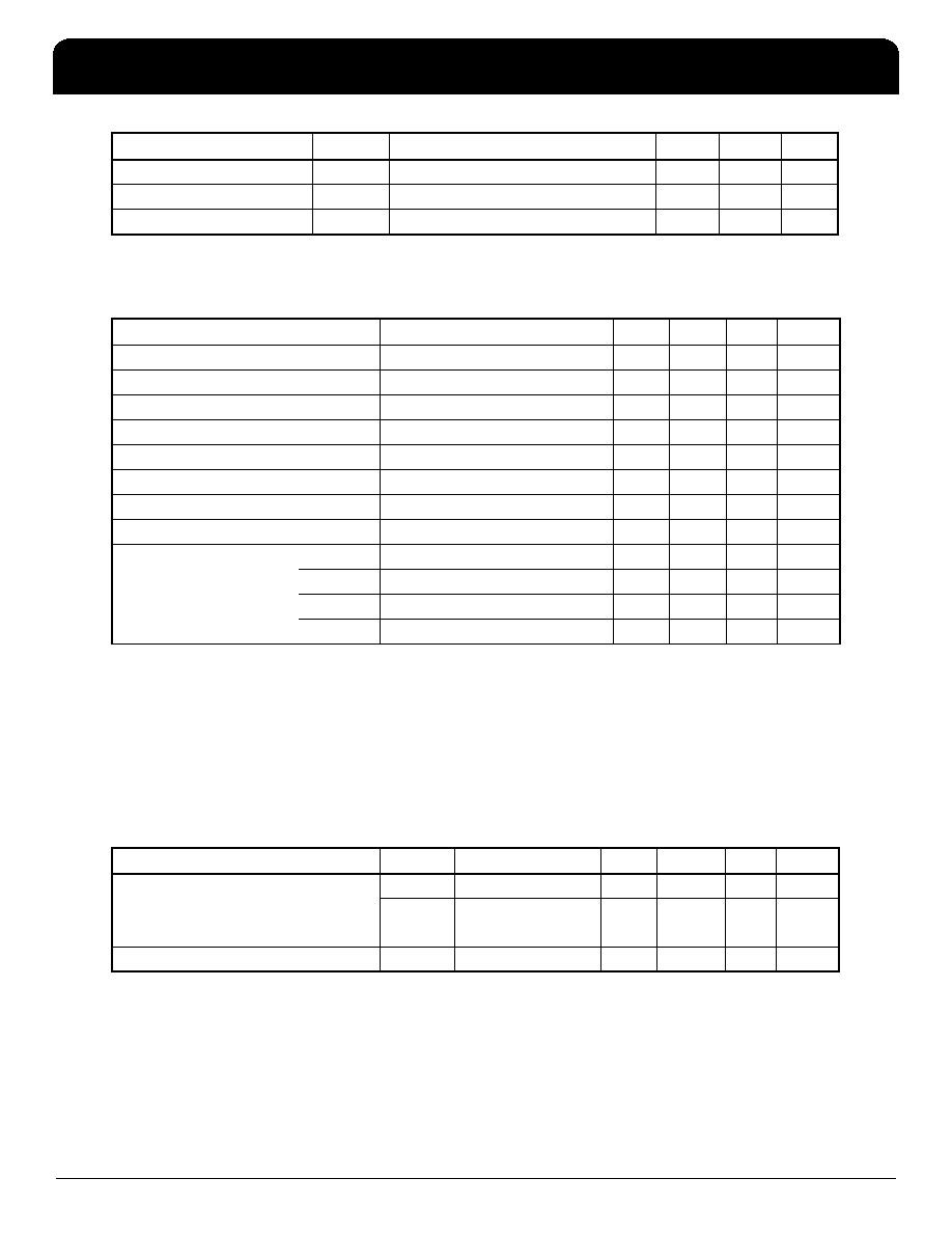
AC Electrical Characteristics
VDD = 3.3V ±10%, Ambient Temperature -40 to +85
° C, unless stated otherwise
Note 1: Rising edge of ICLK compared with rising edge of CLK2, with FBCLK connected to FBIN, and 15 pF load
on CLK2.
Note for OE1
The OE1 pin is intended to facilitate board test. Note that disabling the FBLK will open the loop, causing a
high-frequency to be output from CLK2. Therefore, set OE1 low only if the chip is in power-down (S3:S0 = 0).
Thermal Characteristics
Short Circuit Current
IOS
Each output
±50
mA
Internal Pull-up Resistor
RPU
OE, select pins
200
k
Input Capacitance
CIN
OE, select pins
5
pF
Parameter
Symbol
Conditions
Min.
Typ.
Max.
Units
Parameter
Symbol
Conditions
Min.
Typ.
Max.
Units
Input Clock Frequency
fIN
See table on page 2
5
210
MHz
Output Clock Frequency
210
MHz
Output Rise Time
tOR
0.8 to 2.0 V, no load
1.5
ns
Output Fall Time
tOF
2.0 to 0.8 V, no load
1.5
ns
Output Clock Duty Cycle
tDC
measured at VDD/2
45
50
55
%
Input to Output Skew
Note 1
±100
ps
Maximum Absolute Jitter
short term
±45
ps
Maximum Jitter
one sigma
15
ps
Phase Noise, relative to
carrier, 125 MHz (x5)
100 Hz offset
-103
dBc/Hz
1 kHz offset
-117
dBc/Hz
10 kHz
-111
dBc/Hz
200 kHz
-88
dBc/Hz
Parameter
Symbol
Conditions
Min.
Typ.
Max.
Units
Thermal Resistance Junction to
Ambient
θJA
Still air
120
° C/W
θJA
1 m/s air flow
115
° C/W
θJA
3 m/s air flow
105
° C/W
Thermal Resistance Junction to Case
θJC
58
° C/W
发布紧急采购,3分钟左右您将得到回复。
相关PDF资料
ICS674R-01ILF
IC DIVIDER USER CONFIG 28-SSOP
ICS726ATLFT
IC VCXO 3.3V 12-36MHZ 6-TSOT
ICS810001DK-21LFT
IC CLK GEN SYNC VCXO DL 32VFQFN
ICS81006AKLFT
IC VCXO TO 6 LVCMOS OUT 20VFQFPN
ICS810525AGILF
IC VCXO-LVCMOS/LVTTL 16-TSSOP
ICS813076CYILF
IC VCXO-PLL WIRELESS 64-TQFP
ICS813078BYILF
IC VCXO PLL WIRELESS 64TQFP
ICS813323BGLF
IC ATTENUATOR/MULTIPLIER 24TSSOP
相关代理商/技术参数
ICS670M-04ILFT
功能描述:IC BUFFER/MULTIPLIER ZD 16-SOIC RoHS:是 类别:集成电路 (IC) >> 时钟/计时 - 时钟发生器,PLL,频率合成器 系列:- 标准包装:1,000 系列:- 类型:时钟/频率合成器,扇出分配 PLL:- 输入:- 输出:- 电路数:- 比率 - 输入:输出:- 差分 - 输入:输出:- 频率 - 最大:- 除法器/乘法器:- 电源电压:- 工作温度:- 安装类型:表面贴装 封装/外壳:56-VFQFN 裸露焊盘 供应商设备封装:56-VFQFP-EP(8x8) 包装:带卷 (TR) 其它名称:844S012AKI-01LFT
ICS670M-04IT
功能描述:IC BUFFER/MULTIPLIER ZD 16-SOIC RoHS:否 类别:集成电路 (IC) >> 时钟/计时 - 时钟发生器,PLL,频率合成器 系列:- 产品变化通告:Product Discontinuation 04/May/2011 标准包装:96 系列:- 类型:时钟倍频器,零延迟缓冲器 PLL:带旁路 输入:LVTTL 输出:LVTTL 电路数:1 比率 - 输入:输出:1:8 差分 - 输入:输出:无/无 频率 - 最大:133.3MHz 除法器/乘法器:是/无 电源电压:3 V ~ 3.6 V 工作温度:0°C ~ 70°C 安装类型:表面贴装 封装/外壳:16-TSSOP(0.173",4.40mm 宽) 供应商设备封装:16-TSSOP 包装:管件 其它名称:23S08-5HPGG
ICS670MI-02
功能描述:IC BUFFER/MULTIPLIER ZD 16-SOIC RoHS:否 类别:集成电路 (IC) >> 时钟/计时 - 时钟发生器,PLL,频率合成器 系列:ClockBlocks™ 产品变化通告:Product Discontinuation 04/May/2011 标准包装:96 系列:- 类型:时钟倍频器,零延迟缓冲器 PLL:带旁路 输入:LVTTL 输出:LVTTL 电路数:1 比率 - 输入:输出:1:8 差分 - 输入:输出:无/无 频率 - 最大:133.3MHz 除法器/乘法器:是/无 电源电压:3 V ~ 3.6 V 工作温度:0°C ~ 70°C 安装类型:表面贴装 封装/外壳:16-TSSOP(0.173",4.40mm 宽) 供应商设备封装:16-TSSOP 包装:管件 其它名称:23S08-5HPGG
ICS670MI-02LF
功能描述:IC BUFFER/MULTIPLIER ZD 16-SOIC RoHS:是 类别:集成电路 (IC) >> 时钟/计时 - 时钟发生器,PLL,频率合成器 系列:ClockBlocks™ 标准包装:1,000 系列:- 类型:时钟/频率合成器,扇出分配 PLL:- 输入:- 输出:- 电路数:- 比率 - 输入:输出:- 差分 - 输入:输出:- 频率 - 最大:- 除法器/乘法器:- 电源电压:- 工作温度:- 安装类型:表面贴装 封装/外壳:56-VFQFN 裸露焊盘 供应商设备封装:56-VFQFP-EP(8x8) 包装:带卷 (TR) 其它名称:844S012AKI-01LFT
ICS670MI-02LFT
功能描述:IC BUFFER/MULTIPLIER ZD 16-SOIC RoHS:是 类别:集成电路 (IC) >> 时钟/计时 - 时钟发生器,PLL,频率合成器 系列:ClockBlocks™ 标准包装:1,000 系列:- 类型:时钟/频率合成器,扇出分配 PLL:- 输入:- 输出:- 电路数:- 比率 - 输入:输出:- 差分 - 输入:输出:- 频率 - 最大:- 除法器/乘法器:- 电源电压:- 工作温度:- 安装类型:表面贴装 封装/外壳:56-VFQFN 裸露焊盘 供应商设备封装:56-VFQFP-EP(8x8) 包装:带卷 (TR) 其它名称:844S012AKI-01LFT
ICS670MI-02T
功能描述:IC BUFFER/MULTIPLIER ZD 16-SOIC RoHS:否 类别:集成电路 (IC) >> 时钟/计时 - 时钟发生器,PLL,频率合成器 系列:ClockBlocks™ 产品变化通告:Product Discontinuation 04/May/2011 标准包装:96 系列:- 类型:时钟倍频器,零延迟缓冲器 PLL:带旁路 输入:LVTTL 输出:LVTTL 电路数:1 比率 - 输入:输出:1:8 差分 - 输入:输出:无/无 频率 - 最大:133.3MHz 除法器/乘法器:是/无 电源电压:3 V ~ 3.6 V 工作温度:0°C ~ 70°C 安装类型:表面贴装 封装/外壳:16-TSSOP(0.173",4.40mm 宽) 供应商设备封装:16-TSSOP 包装:管件 其它名称:23S08-5HPGG
ICS67-1
制造商:Thomas & Betts 功能描述:INSULATED SERV.ENTR.SLEEVE 制造商:Thomas & Betts 功能描述:Cable Accessories Compression Splice Aluminum
ICS671-01
制造商:ICS 制造商全称:ICS 功能描述:Zero Delay, Low Skew Buffer and Multipler